Scientific Program

Conference Series Ltd invites all the participants across the globe to attend 30th World Nano Conference Zurich, Switzerland.

Day 1 :

Conference Series Nano 2019 International Conference Keynote Speaker Bernard Pelissier photo
Biography:

After an experience in industrial R&D, Bernard Pelissier integrated CNRS (French National Center for Scientific Research) in 1994. His research activities are mainly focused on material science and surface characterisation. He first worked on massive crystalline growth and MOCVD deposition and then integrated LTM (Laboratoire des Technologies de la Microélectronique) in 2001 as XPS surface characterisation manager. His research interest focused on materials fundamentals studies for process development and contamination studies in clean room. He has been involved in several European collaborative projects in surface characterisation. Since 2005 he is interested in quasi insitu physico chemical characterisation using vacuum transfer. He actually manages the IMPACT Equipex project “A 300mm quasi insitu advanced characterisation platform combining pARXPS, Raman and ellipsometry using vacuum transfer”, dedicated to studies at the frontier between process development studies and upfront research.

Abstract:

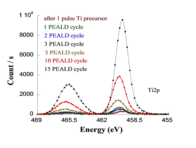
Selective deposition (ASD for Area Selective Deposition) processes are currently a very active topic of study in the microelectronic’s field. Indeed, this type of growth (bottom-up approach) allows to avoid problems of overlays or CD’s variability and mostly to lower costs compared to the classic top-down approaches requiring very complex developments when the dimensions are reduced: multipatterning, or Extreme UV. In this context a selective deposition process of TiO2 on TiN versus Si has been developed at lab [1]. This type of ASD deposition is based on alternating cycles of PEALD (Plasma Ehanced Atomic Layer Deposition) and phases of surface etching / passivation. In this scheme, these phases of passivation can avoid growth on intended areas for a certain number of cycles ALD. In order to understand and control the key steps in these processes during these successive deposit / engraving / passivation cycles, in-situ or quasi in-situ metrologies are valuable tools. They become mandatory when addressing surfaces presenting strong reactivity to air, as in this case here (TiN and Si). This concept of quasi in-situ analysis with mobile vacuum carrier [2] is one of the key facet of the IMPACT project and characterization platform, which has already been validated for many applications (various growth studies, reactive layers in plasma etching, surface functionalization,..) [3, 6]. Thus, after a synthetic description of the platform’s concept and setup the presentation will highlight this specific application for process development of PEALD selective deposition of TiO2 on TiN versus Si. In particular, the study will describe mechanisms involved for these selective growth cycles, and this at the level of the atomic layer, detailing each cycle from the first layers deposited.


Conference Series Nano 2019 International Conference Keynote Speaker Han-Yong Jeon photo
Biography:

Han-Yong Jeon is a Geosynthetics/Technical Organic Materials Researcher and he was the 32nd President of Korean Fiber Society (2014~2015). He has published more than 881 proceedings in domestic and international conferences. He wrote 20 texts including 'Geosynthetics’ and also published 144 papers in domestic and international journals. He has won the awards of Marquis Who's Who-Science and Engineering in 2003~2018 and also, he got the 33rd Academy Award of Korean Fiber Society in 2006 and “Excellent Paper Award of 2012” by The Korean Federation of Science and Technology Societies.


Abstract:

Nanofibers are one of the most advanced materials which can be easily designed with high performance materials having distinctive properties. In addition to fibers, nanoparticles (such as nanoclay) can be used to make unique formulations which can, in turn, be used to make conventional fibers for geotextiles and yarn-type geogrids. As an example of nanocomposite geo-synthetics in geo-environmental applications, it is very important to eliminate the toxic and organic components of various waste leachate solutions. There is no such capability for the standard manufactured nonwoven geotextiles and needed is to manufacture the functional nonwoven geotextiles which can absorb the toxic and organic components that may be harmful to personal health and the environment. The general concept of nanotechnology formulations used to manufacture geotextiles is introduced in this paper. Separation and filtration functions using geotextiles from nanoclay formulations are introduced as an important concept. For an example of nanoclay formulations used to manufacture geotextiles, yellow clay as nanoparticles were added to make a polyester formulation in turn to make nonwoven geotextiles to improve the removal effects of toxic and organic components of leachate solutions. Engineering test behavior was evaluated to confirm the effects of yellow clay addition. Finally, the possibility of nanocomposite formulations for geo-synthetics is considered in a number of common situations.

  • Nanoscience and Technology | Nano Medicine | Nanoparticles | Nano Electronics | Materials Chemistry | Nano Materials Synthesis and Characterisation
Speaker

Chair

Sidorenko Anatolie

Institute of Electronic Engineering and Nanotechnologies, Moldova

Speaker

Co-Chair

Myung Chul Chang

Kunsan National University, South Korea

Session Introduction

Bonamali Pal

Thapar Institute of Engineering and Technology, India

Title: Greener and selective synthesis of various aromatic amines by TiO2 nanocatalyst under light irradiation
Biography:

Abstract:

Photocatalytic reduction of nitro-aromatics to industrially important amino-derivatives using greener process  attracted a great deal of research interest as compared to conventional synthetic techniques. In this context, this research will show some potential usage of different sizes and shapes of bare and metal loaded TiO2, nanostructures (1-4) for the improved photoreduction efficiency of nitroaromatics under solar irradiation. It observed that anisotropic and core-shell nanostructures displaying superior catalysis and photocatalysis properties than conventional bulk catalysts materials. Photocatalytic reduction of 25 μmol 2, 2'-dinitrobiphenyl in 50% aqueous isopropanol and 50 mg P25-TiO2 under an argon atmosphere and 20 h UV light irradiation selectively produced 23.8 μmol of benzo [c] cinnoline (95%), (scheme 1) and 2, 2'-biphenyldiamine (5%) whose amount gradually increased with the irradiation time beyond 20–24 h due to further reduction of benzo [c] cinnoline. Selective photoreduction of mono/dinitro benzene to nitroanline and diaminobenzene etc could be controlled by crystal phases and shapes of TiO2 nanoparticles both under UV and solar irradiation. Highly sunlight photoactive Aloe-veral shaped crystalline rutile TiO2 nanoarchitectures is found to have superior hydrogenation efficiency of different nitroaromatics than conventional P25 and rutile TiO2 under direct sunlight exposure. Cu nanostructures of various shapes and sizes as superior catalysts for nitro-aromatic reduction and co-catalyst for Cu/TiO2 photocatalysis. Likewise core shell and lenghty nanostructures of mono and bimetallic plasmonic nanocatalysts exhibited better selectivity and yield for nitroaromatices reduction.

Biography:

Yoshitaka Okada completed his PhD degree in electronic engineering from the University of Tokyo. He is currently a Professor in the Department of New Energy at the Research Center for Advanced Science and Technology (RCAST) of the University of Tokyo. His recent research interests include epitaxial film growth of low-dimensional quantum nanostructures as well as III-V-N dilute nitrides for applications to high efficient intermediate-band and hot carrier solar cells and multijunction solar cells. Dr. Okada is a member of the IEEE, Materials Research Society (MRS) and Japan Society of Applied Physics (JSAP). He has authored and co-authored over 200 refereed journal publications and over 230 international conference presentations.

Abstract:

Significant efforts have been devoted in order to demonstrate operation of quantum dot intermediate band solar cells (QD-IBSCs) [1]. The challenge for QD-IBSCs is to establish methods to fabricate high-density QDs arrays of low defect density with long carrier lifetimes. The areal density of QDs has direct influence on the generation and recombination processes via IB states since the total density of states of IB (NIB) is linked to the areal density Nareal as NIB = Nareal × Nstacks / W, where Nstacks is the number of QD layer stacks and W is the width QD region, respectively. For this, we have shown that strain-compensated growth improves the QDs quality and characteristics of InAs/GaAs QDSCs with Nstacks up to 100 in self-organized heteroepitaxy by MBE. However, the average QD size prepared by such dry methods is still large and Nareal is low, typically limited to the range of 15-30 nm and 1011- 1012 cm-2, respectively. Furthermore, strain-induced bandgap widening of InAs QDs reduces the offset between the barriers, which results in an increased thermal escape of carriers out of QDs thereby reducing photocurrent production by 2-step photoabsorption (TSPA). In this work, optimization of QD-IBSC structure is studied for which PbS colloidal QDs of 4 nm in size were densely dispersed in a bulk CH3NH3PbBr3 perovskite matrix with a high energy bandgap of 2.4eV [2]. We focus on the TSPA characterization performed at room temperature.
 
Recent Publication
1. Y. Okada et al, Appl. Phys. Rev. 2, 021302 (2015). [2] H. Hosokawa et al, Nature Commun. (2019). DOI:
10.1038/s41467-018-07655-3.

Biography:

Xidong Duan is a Professor at the College of Chemistry and Chemical Engineering, Hunan University, China. His current research interests include twodimensional materials, heterostructures and their applications. He received his BS degree in Chemistry from Hunan University in 1993, his MA degree in Materials from Hunan University in 1996, and his degree in Chemistry from Hunan University in 2016. He was previously a senior engineer at the Changsha Research Institute of Mining and Metallurgy before joining Hunan University.

Abstract:

Two-dimensional layered materials such as garphene, MoS2 and WSe2 have attracted considerable interest in recent times as semiconductor after Si and becoming an important material platform in condensed matter physics and modern electronics and optoelectronics. The studies to date however generally rely on mechanically exfoliated flakes which always be limtited to simple 2D materals, especially 2D lateral complicated structure can not be perpared through exfoliation strategy. Much like the traditional semiconductor technique, complicated structure such as controlling the space distribution of composition and electronic structure of two dimensional semiconductor material is essential to construct all modern electronic and optoelectronic devices, including transistors, p–n diodes, photovoltaic/photodetection devices, light-emitting diodes and laser diodes. And many physics phenomenon can only appear in more complicated structure. To fully explore the potential of this new class of materials, it is necessary to develop rational synthetic strategies of two dimensional lateral complicated struture, such as lateral heterostructure, multiheterostructure, superlattice, quantum well etc., With a relatively small lattice mismatch (~4%) between MoS2 and MoSe2 or WS2 and WSe2, it is possible to produce coherent MoS2–MoSe2 and WS2–WSe2 heterostructures through a lateral epitaxial process (Fig. 1a). Our studies indicate that simple sequential growth often fails to produce the desired heterostructures because the edge growth front can be easily passivated
after termination of the first growth and exposure to ambient conditions. To retain a fresh, unpassivated edge growth front is important for successive lateral epitaxial growth. To this end, we have designed a thermal CVD process that allows in situ switching of the vapour-phase reactants to enable lateral epitaxial growth of single- or few-layer TMD lateral heterostructures. We used this technique to realize the growth of compositionally modulated MoS2– MoSe2 and WS2–WSe2 lateral heterostructures. From the Fig. 1 b,c,d,e we can see the formation of WS2–WSe2 lateral heterostructures clearly. The WS2–WSe2 lateral heterostuctures with both p- and n-type characteristics can also allow us to construct many other functional devices, for example, a CMOS inverter. Fig. 1g is the optical image of the invert constructed using the WS2–WSe2 lateral heterostuctures and the curves of the output–input and the voltage gain. The voltage gain reaches as large as 24.

Biography:

Mirko ÄŒernák is a professor at the Department of Physical Electronics, Faculty of Science, Masaryk University, Brno, Czech Republic. He is also the director of the R&D Centre for Low-cost Plasma and Nanotechnology Surface Modifications (CEPLANT) at Masaryk University. His research interests include the fundamental study of high pressure electrical discharges, plasma chemistry, and applied plasma physics. He has published more than 100 papers in the scientific journals and has been cited more than 2100 times, H-index: 24

Abstract:

Because of their unique properties known only in ceramic materials the mesoporous ceramic nanofibres (CNFs) have been developed for many advanced materials applications in energy harvesting systems, batteries, catalysts, sensors to mention just a few. The usual way to fabricate CNFs consists of a sol-gel electrospinning procedure followed by a thermo-calcination process performed at temperatures up to 800°C for several hours. The slow thermocalcination is the bottleneck in potential in-line or even continuous production, which significantly adds to the cost of CNFs and products manufactured therefrom. An additional problem is that the high calcination temperature is prohibitive in the preparation of inorganic nanofibres layers on heat-sensitive substrates and problematic in adhesion of the nanofibres to metal substrates. A novel fast ambient-air plasma technique enables the calcination at near-room temperatures and times less than 30 min that opens opportunities for the low-cost continuous manufacturing of thin CNFs mats and layers. Moreover to enhance the nanofibres flexibility the plasma calcination enables to manufacture organic/inorganic nanofibres with the core-shell structure. The results on plasma-calcination of TiO2 and Al2O3 CNFs will be presented.

Biography:

Gunther holds an engineer diploma in Chemistry & Plastic technology and bachelor in Safety advisor (2005). With over 10 years of invaluable experience in SHEQ managing projects and resources in an effective and efficient manner. Highly focused with a comprehensive knowledge and understanding of various industries and sectors such as plastic engineering, automotive, trailer building, composite engineering/ development, chemical industry, logistics, Operational services and consulting. As a true professional he is always willing to challenge the status quo and improve on existing standards. Since June 2016 he joined the company OCSiAl as a H&S manager, responsible for the regulatory affairs worldwide.

Abstract:

The company OCSiAl is been founded in 2009 and is also the first SWCNT manufacturer who has completed his EU-REACH registration for a tonnage band of up to 10T/a and is planning to receive approval for a tonnage band up to 100T/y by the end of Q3/2019. At the end of the 2017 we achieved our signed consent order with the EPA that allows us to import up to 25T/y. Because Tuball™ is used and also tested in various applications on an ongoing basis, also receiving a lot of interests worldwide. That is why it is obvious that the company OCSiAl is establishing the necessary regulatory and quality standards worldwide. The first part of this presentation will aim at providing a short introduction of our Tuball™ substance and his product line, a second part of the presentation will be about the morphology vs Health & Safety status, the third part is an overview about the status and plans of the ongoing registrations an compliance. The fourth and last part of the presentation will focus on the health, safety and environmental aspects of our Tuball™ substance and the different applications. As SWCNT manufacturer, OCSiAl is doing continues investments in improving our understanding of our different (new) Tuball products themselves and potential hazards through their (entire) life cycle. We are involved in generating additional test data and collaborating with industry associations and networks. This presentation will describe the steps being taken by the company’s H&S Lead manager, Van Kerckhove Gunther to successfully introduce our carbon nanotubes (SWCNT’s) regulatory status and outline our (future) plans for numerous of studies and qualifying our Tuball™ substance including the different kind of compositions.

Biography:

Elisabetta Travaglia is a research fellow at CNR-IOM Trieste, working within the H2020 European project NFFA Europe, where she deals with the technical aspects of transnational access to the laboratories, and actively takes part to the management of the whole project. Elisabetta has a master degree in Chemistry and a PhD degree in Nanotechnology, both obtained at the University of Trieste. Since several years she has been involved in dissemination and outreach activities both for experts and general public, also addressing children to show them that science is fun.

Abstract:

NFFA-Europe is a European open-access resource for experimental & theoretical nanoscience that carries out comprehensive projects for multidisciplinary research at the nanoscale ranging from synthesis to nanocharacterization, to theory and numerical simulation. Advanced infrastructures specialized on growth, nano-lithography, nano-characterization, theory and simulation and fine-analysis with Synchrotron, FEL and Neutron radiation sources are integrated into a multi-site combination to develop frontier research on methods for reproducible nanoscience research thus enabling European and international researchers from diverse disciplines to carry out advanced proposals impacting on science and innovation. NFFA-Europe coordinates access to infrastructures on different aspects of nanoscience research that are not currently available at single specialized sites without duplicating specific scopes. Internationally peer-reviewed approved user projects have access to the best suited instruments, competences and technical support for performing research, including access to analytical large scale facilities, theory and simulation and high-performance computing facilities. Access is offered free of charge to European users. Two researchers per user group are entitled to receive partial financial contribution towards the travel and subsistence costs incurred. The user access scheme includes at least two “installations” and is coordinated via a single entry point portal that activates an advanced user-infrastructure dialogue to build up a personalized access programme with an increasing return on science and innovation production. NFFA-Europe’s own research activity addresses key bottlenecks of nanoscience research: i.e. nanostructure traceability, protocol reproducibility, in-operando nano-manipulation and analysis, open data.